
 點擊圖片放大
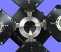
MultiView 4000
Multi-Probe Optically Integrated AFM-Raman-NSOM
MultiView 4000
Multi-Probe Optically Integrated AFM-Raman-NSOM
以色列 NANONICS 是業界將近場光學顯微鏡 (NSOM) 技術和原子力顯微鏡 (AFM) 技術相結合的領導品牌,亦是對此類產品經驗最豐富的公司之一。加上其強大的系統整合能力,將所有的材料表徵分析整合在一個實驗平臺上,並能即時或同時進行下列數種成像分析實驗包括:
★同步式多探針掃描成像
最多四組探針組
★ 近場掃描光學顯微影像
★ 原子力顯微影像
★ 共軛焦顯微影像
★ 奈米級熱電偶溫度成像
★ 奈米級熱阻抗成像
★ 奈米級電子導電度成像
★ 表面能與表面功函數成像
★ 奈米級壓電力成像
★ 奈米級磁力成像 (可變磁力控制)
★ 奈米級電子力成像
★ 奈米級掃描電化學顯微成像 (SECM)
★ 針尖增強拉曼散射成像 (TERS)
★ 原子力顯微鏡結合掃描電子顯微鏡
★ 原子力顯微紅外光、太赫茲光源與拉曼散射成像


近場光學實驗 ↓


Up to 4 AFMs in One System
- • Four probes operate simultaneously and independently, with each probe having its own feedback and scanning capabilities.
- • Measure sophisticated properties only possible with the availability of multiple probes such as electrical, thermal and optical properties of devices
- • The MultiView 4000is a novel platform containing multiple probes/AFM's for advanced experiments such as: nanoscale transport, optical pump-probe, read-write experiments.
The MV 4000 continues the tradition of the MV series of providing total optical flexibility and customization possibilities so that now AFM Raman and tip enhanced Raman spectroscopy (TERS) can be integrated with the multiprobe capability. Finally, free optical access from above allows easy visualization of all probes and facilitates nanomanipulation.
The MV 4000 product brochure can be downloaded here.
The simultaneous and independent SPM probe operation of up to 4 probes enables full characterization of all dimensions of samples and devices. All forms of SPM are enabled for each individual probe accompanied by total optical integration resulting in access to all modes including AFM, KPM, EFM, ANSOM, NSOM, STM, AFM-Raman, and TERS. Because these probes are designed for multiple probe operation, they can be brought to a nanometric separation distance thus ensuring that the same area is scanned with all the probes.
Multiprobe capability is especially useful for electrical measurements since multiple probes can now be placed over the element to provide bias or probe its conductivity, resistance, etc just like in a probe station. Two-, three-, or four-point resistance measurements are possible. Multiple probes also enable flexible positioning and manipulation to provide bias, localized I-V measurements, and multichannel imaging.
One probe can be the source of excitation while the second probe follows the transport process with high spatial resolution. Alternatively, optical pump/probe experiments can now be performed using one probe to optically pump while the other probe measures the optical output in a variety of configurations. An example of each type of measurement is shown below.
Thermal transport measurement within an SRAM device where heat is introduced at specific locations and detected at other locations. As contact is made in different regions of the SRAM with the thermal conductivity probe, the probe tip cools to different levels depending on the material's thermal conductivity. The resulting image is obtained by determining the current alterations that had to to be affected in order to keep the current flowing past the point resistance at a constant value.
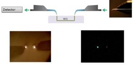
With two cantilever, near-field optical probes with exposed tips, light is injected through one probe and is guided through the sample which is a fiber. With the second probe in place, this injected light can be collected and analyzed both spatially and temporally. In this image two NSOM probes are seen in AFM contact with the input and output of the fiber waveguide.
See a video showing an example using multiprobe technology to conduct nanothermal measurements here.
With a multiprobe system, resolution and tip quality no longer need to be compromised since each probe is now individualized for each measurement. In classic NSOM setups the NSOM probe would have the dual function of imaging topography and fluorescence where the topography image is compromised by the aperture (wider diameter) needed by the NSOM probe. But in a multiprobe setup, a standard SPM probe can be used the topography without affecting the NSOM fluorescence measurement.

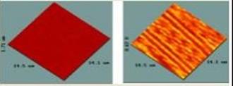
The left and center images are the topography and fluorescence images, respectively, of lumogen dye particles collected in a multiprobe setup with different probes for topography and NSOM. The image on the right is the topography image of the same sample but collected with the NSOM probe, revealing the clear loss of resolution and morphology. The width of each image is 8um.
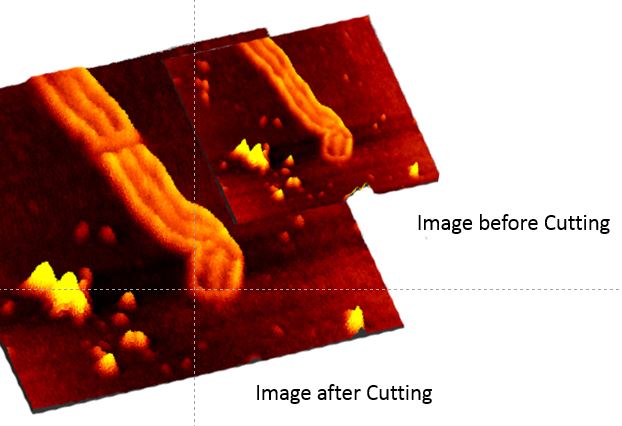
One probe can be used for moving, cutting, or positioning a sample, while the other probe can be used to image the sample. For example, shown below is a chromosome that has been dissected with one probe (see image on left), while the other probes images the result of the nanomanipulation.
|
|
|
(Left) MultiView 4000TM four SPM probes platform. (Middle) MultiView 4000TM Tip and | ||
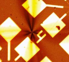
The images above show the procedure that can be implemented to bring two or more probes in close proximity to one another. Specifically in the images shown the common features in a carbon nanotube sample are imaged by two probes and from these images it is clear that the two probes are displaced along the y axis by 300nm and along the x axis by 1.7microns |
更多商品

CryoViewTM 2000
以色列 NANONICS 是業界將近場光學顯微鏡 (NSOM) 技術和原子力顯微鏡 (AFM) 技術相結合的領導品牌,亦是對此類產品經驗最豐富的公司之一。加上其強大的系統整合能力,將所有的材料表徵分析整合在一個實驗平臺上,並能即時或同時進行下列數種成像分析實驗包括: ★ 近場掃描光學顯微影像 ★ 原子力顯微影像 ★ 共軛焦顯微影像 ★ 奈米級熱電偶溫度成像 ★ 奈米級熱阻抗成像 ★ 奈米級電子導電度成像 ★ 表面能與表面功函數成像 ★ 奈米級磁力成像 (可變磁力控制) ★ 奈米級電子力成像 ★ 奈米級掃描電化學顯微成像 (SECM) ★ 原子力顯微拉曼散射成像 ★ 針尖增強拉曼散射成像 (TERS) ★ 溫度變化控制,最低可達10K 可於腔體內進行臨場變溫實驗分析,最低溫可達10K ↓
MultiView 1000
以色列 NANONICS 是業界將近場光學顯微鏡 (NSOM) 技術和原子力顯微鏡 (AFM) 技術相結合的領導品牌,亦是對此類產品經驗最豐富的公司之一。加上其強大的系統整合能力,將所有的材料表徵分析整合在一個實驗平臺上,並能即時或同時進行下列數種成像分析實驗包括: ★ 近場掃描光學顯微影像 ★ 原子力顯微影像 ★ 共軛焦顯微影像 ★ 奈米級熱電偶溫度成像 ★ 奈米級熱阻抗成像 ★ 奈米級電子導電度成像 ★ 表面能與表面功函數成像 ★ 奈米級壓電力成像 ★ 奈米級磁力成像 ★ 奈米級電子力成像 ★ 奈米級掃描電化學顯微成像 (SECM) ★ 原子力顯微拉曼散射成像 MultiView 1000 Entry-level system with optical capability upgrade The award winning MultiView 1000TM is an entry-level system that fully integrates all forms of scanning probe microscopy (SPM) with conventional optical microscopy. The MultiView 1000 system provides a cost-effective SPM solution complete with advanced SPM features. The design of the MultiView 1000 emphasizes ease-of-use so that customers with any technical background can quickly make SPM measurements. This system can also be easily upgraded to more sophisticated measurements such as NSOM and AFM-Raman. MV 1000 Product brochure can be downloaded here Unprecedented flexibility and performance Ease of use designed for quick setup with any background. Compatible with NanoToolKit of probes including all third party silicon probes. Easily upgradable to perform sophisticated measurements including AFM-Raman and NSOM Standard packages include magnetic force microscopy (MFM) and electrostatic force microscopy (EFM); more advanced modes including kelvin force microscopy and scanning capacitance microscopy available in an upgrade Complete optical access to scanning probe microscopy head Unique geometry leaves the optical axis free both above and below the sample for integration with upright, inverted, and dual optical (both upright and inverted) microscopy configurations Accomodates wide variety of probes Nanonics provides a wide variety of probes that are compatible with the MultiView 1000 including glass, cantilevered probes, thermal probes, electrical and magnetic probes (electrochemical probes, coax probes, glass insulated wire probes), all third party silicon probes, chemical writing probes Largest Commercially Available Z Scan Range The large 85 micron x,y, and z-range of the Nanonics 3D Flatscan makes it ideal for optical sectioning in confocal imaging. Used in this way, the MultiView 1000 integrates conventional far-field imaging, confocal microscopy, AFM, and near-field optics in a single system. Overall, the MultiView 1000 is a robust and versatile SPM system that allows the user to zoom, with overlapping fields of view, from the lowest resolution of conventional far-field imaging to the higher resolution of confocal microscopy, and finally, to the ultimate resolution of AFM and NSOM.
MultiView 2000 Advanced, Fully Featured SPM
以色列 NANONICS 是業界將近場光學顯微鏡 (NSOM) 技術和原子力顯微鏡 (AFM) 技術相結合的領導品牌,亦是對此類產品經驗最豐富的公司之一。加上其強大的系統整合能力,將所有的材料表徵分析整合在一個實驗平臺上,並能即時或同時進行下列數種成像分析實驗包括: ★ 近場掃描光學顯微影像 ★ 原子力顯微影像 ★ 共軛焦顯微影像 ★ 奈米級熱電偶溫度成像 ★ 奈米級熱阻抗成像 ★ 奈米級電子導電度成像 ★ 表面能與表面功函數成像 ★ 奈米級磁力成像 ★ 奈米級電子力成像 ★ 奈米級掃描電化學顯微成像 (SECM) ★ 原子力顯微拉曼散射成像 ★ 針尖增強拉曼散射成像 (TERS) ★ 原子力顯微鏡結合掃描電子顯微鏡 Advanced, Fully Featured SPM The MultiView 2000TM series is an advanced single probe scanning probe microscope enabling a variety of modes of AFM/SPM/NSOM imaging. Nanonics has designed The MultiView 2000TM for excellence in scanning probe microscopy while allowing for near-field and far-field optical NSOM/AFM Raman/TERS imaging without perturbation. The Multiview 2000TM is the only commercially available instrument that offers both tip and sample scanning. This versatility is important for different operation modes where the user can now choose whether the sample or tip is static. The Multiview 2000TM further offers the most stable feedback mechanism available in the form of normal force feedback with tuning fork actuation. This feedback mechanism offers the most stability, as well as laser-free operation for the most sensitive experiments. The MV 2000TM product brochure can be downloaded here. Designed for Ease-of-Use and Flexibility Dual sample and tip scanning stages in the same head for ultimate flexibility is coupled with an optically friendly Nanonics 3D Flat ScanTM stage providing up to 85μ in X, Y and Z or 170μ in X, Y and Z using combined scanners. This scanner is also suitable for large samples with unconventional geometries. Closed loop is an option for positioning accuracy of 20nm. Additionally, a revolutionary, alignment-free feedback system provides the most sensitive tip-sample stability. Normal force feedback with tuning fork actuation provides no alignment, laser-free operation for improved optical signal to noise ratio, and ultra-sensitive force spectroscopy perfect for force and adhesion measurements. Read more for more information and details about tuning fork feedback Largest Commercially Available Z Range The large, 85μ X, Y and Z-range of the Nanonics 3D FlatscanTM makes it ideal for optical sectioning in confocal imaging. Used in this way, the MultiView 2000TM integrates conventional far-field imaging, confocal microscopy, AFM, and near-field optics in a single system Excellent SPM platform compatible with wide variety of probes Nanonics provides a wide variety of probes that are compatible with the MultiView 2000TM, including: transparent, cantilevered probes, thermal probes, electrical probes (electrochemical probes, coax probes, glass insulated wire probes) and all third party silicon probes Any Optical Configuration The unique geometry of the MultiView 2000TM head and cantilever probes leaves the optical axis free both above and below the sample for integration with upright, inverted, and dual optical microscope configurations. Irregular Sample Size Compatibility Irregular sample sizes, whether odd in shape or large in size, can be easily placed on the sample stage. The sample can even be suspended from the unobstructed flat scanning sample stage in order to examine the edges of the sample.
SpectraView MV2500
以色列 NANONICS 是業界將近場光學顯微鏡 (NSOM) 技術和原子力顯微鏡 (AFM) 技術相結合的領導品牌,亦是對此類產品經驗最豐富的公司之一。加上其強大的系統整合能力,將所有的材料表徵分析整合在一個實驗平臺上,並能即時或同時進行下列數種成像分析實驗包括: ★ 近場掃描光學顯微影像 ★ 原子力顯微影像 ★ 共軛焦顯微影像 ★ 奈米級熱電偶溫度成像 ★ 奈米級熱阻抗成像 ★ 奈米級電子導電度成像 ★ 表面能與表面功函數成像 奈米級壓電力成像 ★ 奈米級磁力成像 (可變磁力控制) ★ 奈米級電子力成像 ★ 針尖增強拉曼散射成像 (TERS) ★ 原子力顯微紅外光、太赫茲光源與拉曼散射成像 ←奈米級磁力成像 (可變磁力控制)分析裝置 原子力顯微紅外光、太赫茲光源與拉曼散射成像分析裝置 ↓ A Breakthrough in Combining Complementary Scattering Techniques with Ultrasensitive AFM and SPM for NanoChemical Analysis • Colocalized IR, Raman, THz and AFM • Singular protocols for excitation in the IR with Raman and fluorescence detection in the visible • Image with photon force with pN force sensitivity • Patented cantilevered completely transparent probes • Highly localized scattering at the tip • Versatile configurations with advanced SPM modes of operation: Kelvin Probe chemical potential, electrical, thermal and photon force detection • Online variable magnetic fields • Applications in plasmonics of 2D materials, liquids, biology etc. AFM (Left) and IR (right) images obtained with broadband IR illumination (1000-4000cm-1) at the MIRIAM beamline of the Diamond Light Source, Harwell, United Kingdom
